

Executive Summary
- The Core Announcement: Nvidia introduced a comprehensive AI and digital twin architecture built on Omniverse and CUDA-X libraries designed to transform semiconductor fabrication facilities.
- Industrial Partnerships: Global chipmakers and equipment leaders including TSMC, Micron Technology, Lam Research, Synopsys, Siemens, and KLA are integrating the platform into cleanroom engineering workflows.
- Physics-Driven Simulation: Debuted cuPotential, a specialized CUDA-X acceleration library that speeds up molecular dynamics and atomic interaction models for sub-2nm transistor gate geometries.
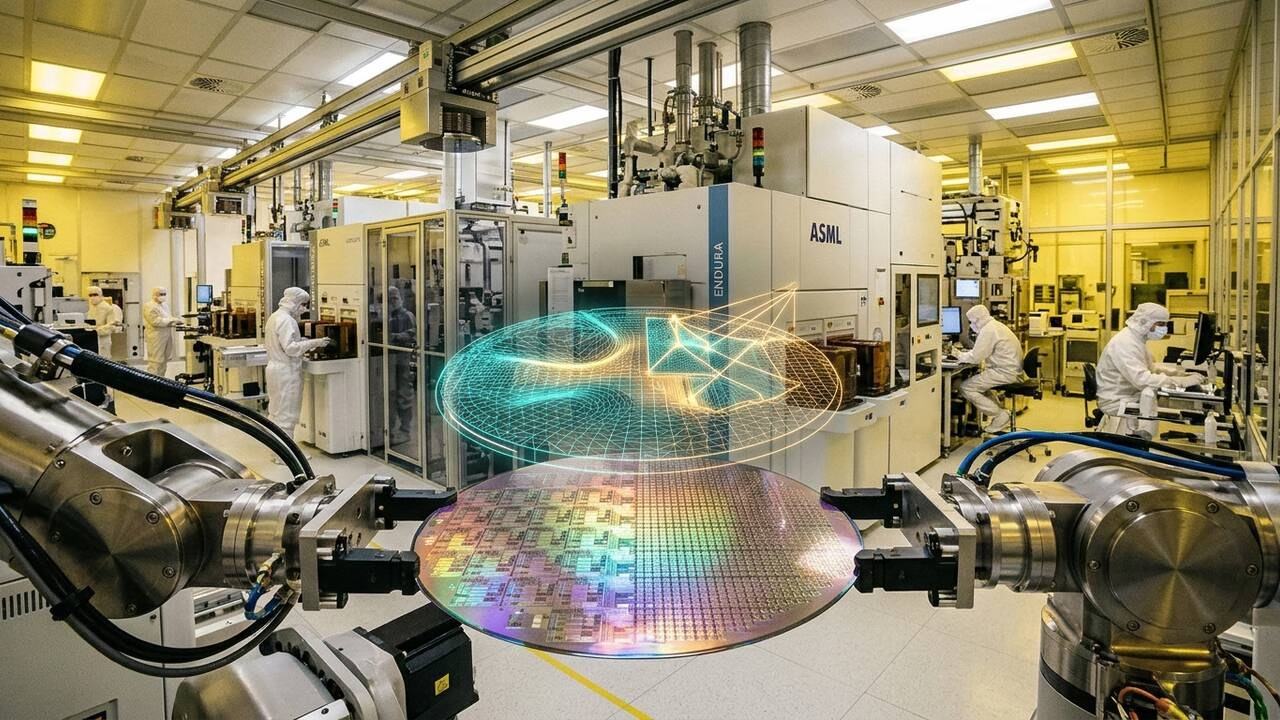
- Virtual Cleanroom Twins: Enables chip manufacturers to simulate automated material handling systems (AMHS), robotic wafer transport, and airflow dynamics inside digital replicas before altering physical billion-dollar production lines.
- Manufacturing Yield Optimization: Combines GPU-accelerated inverse lithography (cuLitho) and edge computer vision to detect microscopic silicon defects in real time during production runs.
Table of Contents
- The Escalating Physics Crisis of Advanced Semiconductor Fabs
- Inside Omniverse Digital Twins: Simulating Cleanroom Robotics
- cuPotential: Accelerating Atomic-Scale Materials Science
- Computational Lithography and Real-Time Defect Detection
- Industry Adoption: TSMC, Micron, and Equipment Builders
- Technical Comparison: Legacy Fab Operations vs AI Digital Twin Fabs
- Frequently Asked Questions
The Escalating Physics Crisis of Advanced Semiconductor Fabs
Constructing a leading-edge semiconductor fabrication facility now costs upwards of $20 billion. Inside these massive facilities, thousands of automated machines process 300mm silicon wafers across hundreds of chemical, thermal, and optical steps. As transistor dimensions shrink below two nanometers toward the angstrom era, physical margins for error have vanished.
At these dimensions, quantum tunneling, atomic migration, and microscopic thermal variances dictate whether a wafer yields functioning microprocessors or expensive scrap. Reconfiguring cleanroom tooling or testing factory layout changes on live production lines risks halting operations that generate millions of dollars in output every hour.
To eliminate this physical bottleneck, Nvidia has introduced an AI-defined architecture for semiconductor fabs. By merging physics-based digital twins, accelerated molecular chemistry libraries, and real-time edge vision, the technology enables foundries to model, test, and optimize every aspect of cleanroom operations virtually before executing physical alterations.
This push coincides with extraordinary computing demand across the tech sector. As documented in our report on how Revolut deployed 56 Nvidia B200 GPUs to cut AI coding costs by 90%, hyperscale inference relies entirely on advanced silicon packaging. Scaling silicon production requires software that can simulate microscopic cleanroom physics with mathematical precision, paralleling advanced modeling techniques showcased in Nature Genetics research on pediatric brain tumor therapy.
Inside Omniverse Digital Twins: Simulating Cleanroom Robotics
The foundation of Nvidia fab platform rests on Nvidia Omniverse, the computing platform for building OpenUSD-based industrial digital twins. Rather than working with disconnected 2D CAD drawings and statistical spreadsheets, manufacturing engineers can construct full-scale, physics-accurate 3D simulations of complete mega-fabs.
Within these digital replicas, plant engineers simulate complex operational dynamics:
- Automated Material Handling Systems (AMHS): Overhead hoist transport vehicles carry Front Opening Unified Pods (FOUPs) filled with silicon wafers along suspended rail networks. Digital twins model vehicle congestion, track switches, and routing bottlenecks under peak wafer production scenarios.
- Cleanroom Airflow and Thermal Dynamics: Simulates laminar air currents and temperature gradients across thousands of square meters, ensuring that heat produced by high-power extreme ultraviolet (EUV) lithography scanners does not cause microscopic wafer warpage.
- Ergonomics and Safety Validation: Models technician movement alongside autonomous mobile robots (AMRs) using Nvidia Isaac Sim, verifying collision avoidance protocols prior to equipment deployment.
By simulating layout changes in Omniverse, foundries can test modifications to equipment clusters, reducing physical qualification downtime by weeks.
cuPotential: Accelerating Atomic-Scale Materials Science
Beyond macro-level factory logistics, modern semiconductor manufacturing requires modeling interactions at the atomic scale. Advanced gate-all-around (GAA) nanosheet architectures and backside power delivery networks rely on exotic chemical films only a few atoms thick.
To address this challenge, Nvidia unveiled cuPotential, a high-performance library within the CUDA-X catalog. The software accelerates interatomic potential calculations used in molecular dynamics and density functional theory (DFT) simulations:
- Orders-of-Magnitude Speedup: Delivers significant acceleration over CPU-based molecular modeling, cutting simulation times for chemical vapor deposition (CVD) and atomic layer etching (ALE) from months to days.
- Defect Mechanism Modeling: Allows materials scientists to simulate how copper interconnects, cobalt barriers, and low-k dielectrics interact under high electrical and thermal stress over years of operation.
- Partner Integrations: Works alongside electronic design automation tools from Synopsys and multiphysics software from COMSOL, giving research teams a cohesive pipeline from atomic modeling to chip layout.
Computational Lithography and Real-Time Defect Detection
Manufacturing chips with sub-2nm features requires extreme ultraviolet light to print microscopic patterns on silicon wafers. Because light diffracts at such small scales, foundries use inverse lithography technology (ILT) to mathematically calculate inverted photomask shapes that produce the desired pattern on the wafer.
Nvidia cuLitho software library shifts this computational burden from massive CPU clusters to GPU acceleration. Foundries can calculate complex inverse lithography masks up to 40 to 60 times faster, reducing the data center footprint needed for mask synthesis from thousands of server nodes to compact GPU systems.
In parallel, Nvidia edge AI models power Automated Optical Inspection (AOI) systems built by partners like KLA and Lam Research:
- Nanometer Particle Spotting: High-speed computer vision models inspect wafer surfaces at line rate, identifying microscopic chemical residues and bridge defects that escape traditional rule-based optical inspection.
- Root Cause Correlation: Connects real-time defect telemetry back to specific process chambers, allowing engineers to service faulty gas valves or plasma sources before multiple wafer batches suffer yield loss.
This high-speed processing directly connects to broader cloud compute developments. As highlighted in our analysis of Fal.ai scaling custom AI inference infrastructure, low-latency model execution is reshaping modern engineering pipelines from consumer apps down to physical silicon manufacturing.
Industry Adoption: TSMC, Micron, and Equipment Builders
The transition toward AI-defined fabs is supported by leading semiconductor manufacturers and tool providers:
- TSMC: Leverages cuLitho and GPU acceleration to speed up mask synthesis for advanced nodes, optimizing manufacturing cycle times.
- Micron Technology: Employs Omniverse digital twin models across its memory fabrication cleanrooms to optimize wafer logistics and accelerate high-bandwidth memory (HBM3e and HBM4) production.
- Lam Research and KLA: Integrate Nvidia accelerated computing libraries into plasma etching, deposition, and wafer metrology equipment, delivering inline telemetry processing.
- Siemens and Synopsys: Connect industrial automation and digital twin software to Omniverse, enabling end-to-end simulation from circuit design to physical factory floor operations.
Technical Comparison: Legacy Fab Operations vs AI Digital Twin Fabs
The factsheet below highlights the core technological differences between traditional cleanroom management and Nvidia AI-defined digital twin architecture:
| Operational Dimension | Traditional Cleanroom Architecture | Nvidia AI Digital Twin Platform |
|---|---|---|
| Fab Layout Testing | Static 2D CAD models; physical trial runs on production floor | Full physics-based 3D digital twins in Omniverse with OpenUSD |
| Photomask Synthesis | CPU server farms running weeks of numerical calculations | GPU-accelerated cuLitho delivering 40x to 60x faster mask calculations |
| Atomic Materials Modeling | Slow DFT simulations limited to small molecular clusters | cuPotential acceleration for large-scale atomic interaction models |
| Defect Inspection | Rule-based optical inspection with delayed manual review | Real-time edge AI vision spotting nanoscale flaws inline |
| Robotic Transport Management | Fixed track schedules with limited dynamic re-routing | Autonomous mobile robots and AMHS coordinated via Isaac Sim |
Frequently Asked Questions
1. What is an AI-defined semiconductor fab?
An AI-defined semiconductor fab is a microchip manufacturing plant that uses real-time physics simulation, digital twin software, and computer vision to design cleanroom layouts, simulate automated material transport, accelerate lithography, and detect wafer defects during production.
2. What role does Nvidia Omniverse play in chip factories?
Omniverse provides the 3D graphics and physics engine for building full-scale digital replicas of cleanrooms. It lets engineers model automated material handling vehicles, cleanroom airflow, and robotic operations virtually, avoiding costly downtime on physical production lines.
3. What is cuPotential and how does it help chip design?
cuPotential is an accelerated CUDA-X library that speeds up molecular dynamics and atomic interaction calculations. It allows materials scientists to model chemical vapor deposition and atomic layer etching at the atomic level, assisting in the development of sub-2nm transistor structures.
4. How does cuLitho improve semiconductor lithography?
cuLitho accelerates inverse lithography computations using GPU clusters rather than thousands of CPU servers. It computes complex photomask shapes up to 60 times faster, significantly lowering data center power consumption and manufacturing preparation time for extreme ultraviolet lithography.
5. Which semiconductor companies are using this platform?
Key semiconductor leaders adopting Nvidia fab software and acceleration libraries include foundry giant TSMC, memory manufacturer Micron Technology, and equipment makers such as Lam Research, KLA, Siemens, and Synopsys.








[…] telecommunications milestone connects to the broader industrial automation landscape. Just as Nvidia deploys AI digital twins across semiconductor cleanrooms, major network operators are replacing manual human intervention with autonomous, self-optimizing […]