
Table of Contents
The global semiconductor sector is entering an expansive phase where total annual revenues are now projected to surpass the significant $1.5 trillion milestone by the year 2030. This immense structural growth is fueled primarily by the rising requirements of high-performance computing and the rapid integration of artificial intelligence into modern data center architectures. TSMC Senior VP Kevin Zhang noted that AI demand has surprisingly overtaken smartphones and IoT devices as the primary driver for advanced silicon production across the industry.
This pivot toward AI-centric infrastructure as the foundation for digital applications requires a structural pivot in foundry capacity allocation and logic design across the global landscape. These escalating market pressures have led directly to the urgent development of a new generation of logic technology designed specifically to handle massive computational artificial intelligence workloads.
Technical Benchmarks for Next-Generation Logic Density and Power Efficiency
The upcoming A14 process represents a vital strategic milestone as the official successor to the industry-leading N2 node, which begins high-volume production later this calendar year. This advanced technology will provide essential hardware foundations for complex transistor architectures required to support the power-intensive workloads of modern generative artificial intelligence and high-performance computing.
Technical benchmarks indicate the A14 node will deliver either a fifteen percent increase in speed or a thirty percent reduction in total power consumption for foundry customers. Furthermore, the new logic process technology will offer a twenty percent increase in density, allowing more compute units to be integrated within the same physical footprint.
- TSMC plans to begin manufacturing advanced chips for primary AI customers like Nvidia using the base A14 process technology starting within the 2028 high-volume production timeline.
- The 2029 arrival of A13 and A12 enhancements will include a six percent reduction in chip size specifically for the A13 variant compared to the initial node.
- Engineers will introduce the Super Power Rail backside power scheme for the A16 node in 2026 and later integrate this technology into derivative A14 versions by 2029.
These individual transistor-level gains must be supported by revolutionary physical integration and advanced packaging technologies to ensure that total system performance continues to scale effectively over time. Consequently, the focus of innovation is shifting from simple lithographic dimensions toward the comprehensive integration of complete systems within a single high-performance semiconductor package or wafer.
Advanced Packaging as the New Driver for System Density
Advanced packaging is now recognized as the primary enabler of density gains because traditional lithographic scaling is facing increasingly difficult physical limits and escalating economic production barriers. Leading manufacturers are prioritizing sophisticated integration schemes that allow for the combination of multiple logic tiles and high-bandwidth memory within a single, highly efficient compute system.
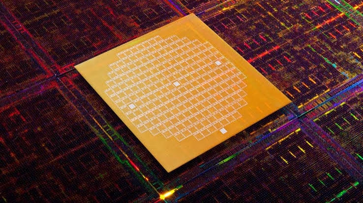
The System-on-Wafer technology described by Kevin Zhang utilizes a full 300-mm wafer as a base, providing forty times the reticle size for massive physical component integration. Companies like Cerebras have already leveraged this wafer-level integration to bring numerous compute dies together, creating a unique and competitive architecture for large-scale artificial intelligence model training. Technologies like CoWoS and 3D stacking of small outline integrated circuits allow for high-density compute clusters to be surrounded by high-bandwidth memory for maximum data throughput.
TechInsights vice chair Dan Hutcheson suggests that TSMC’s system-integration density gains are effectively reviving Moore’s Law through innovative packaging rather than relying solely on simple lithographic scaling. These architectural milestones require specific lithographic tools and cost-management strategies to ensure the production of these massive silicon systems remains financially viable for most global technology customers.
The High-NA EUV Transition and the 12-Inch Mask Initiative
Significant strategic tension exists between adopting extremely expensive new lithography tools and maintaining cost-effective production for the advanced transistor architectures required by global artificial intelligence chip customers. Foundries must carefully balance the performance benefits of early hardware adoption against the potential for increased manufacturing complexity and significantly higher capital expenditures for their primary design partners.
TSMC and Intel have adopted contrasting High-NA EUV strategies, with TSMC planning to delay full adoption until the sub-1-nm era to minimize mask increases and process complexity. This cautious approach allows TSMC to leverage existing multi-patterning expertise on current low-NA systems while providing more affordable and stable manufacturing solutions for its high-volume foundry customers.
A collaborative initiative between ASML and TSMC aims to transition to 12-inch photomasks by establishing a pilot production line in 2031 to increase fab productivity and efficiency. ASML CEO Christophe Fouquet stated that the transition from 6-inch to 12-inch masks will eventually support full High-NA system readiness for advanced semiconductor production nodes by 2033. This focus on manufacturing efficiency leads directly toward the emerging role of light-based communication to solve power and latency bottlenecks currently facing modern high-performance artificial intelligence centers.
Solving Data Center Crises With COUPE Technology
Silicon photonics is now a strategically vital technology for mitigating the soaring power demands and grid stress caused by the rapid expansion of global artificial intelligence data centers. By integrating light-based signaling directly into the processor architecture, designers can significantly reduce the energy lost during data transmission between various compute and memory components in the system.
The Compact Universal Photonics Engine will replace power-hungry copper interconnects with light-based signaling to improve energy efficiency and reduce signal latency across high-performance compute clusters and fabrics. Integrating compute tiles with these optical engines via CoWoS can achieve a two-fold latency reduction and a two-and-a-half-fold improvement in the total power efficiency of interconnects. While smaller rivals like GlobalFoundries and Tower Semiconductor entered the silicon photonics market earlier, TSMC plans to roll out its own specialized production platform within the next calendar year.
This holistic strategy ensures that the foundry remains the indispensable partner for every major technology firm seeking to build the future of autonomous and generative artificial intelligence. TSMC’s integrated roadmap and technological leadership position the company to dominate the $1.5 trillion semiconductor market by delivering the performance and efficiency required for the 2030 horizon.